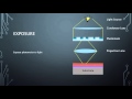
Sam Sivakumar of Intel talks about Lithography and Patterning: Part 1
Sam Sivakumar of Intel talks about Lithography and Patterning
- Scaling of Wavelength
- Double Patterning
Видео Sam Sivakumar of Intel talks about Lithography and Patterning: Part 1 канала nanolearning
- Scaling of Wavelength
- Double Patterning
Видео Sam Sivakumar of Intel talks about Lithography and Patterning: Part 1 канала nanolearning
Показать
Комментарии отсутствуют
Информация о видео
Другие видео канала
 Sam Sivakumar of Intel talks about Lithography and Patterning: Part 2
 Double Patterning to the rescue (LELE, LFLE, SADP) - Part 1
 Erik Loopstra & Vadim Banine - Extreme ultraviolet lithography
 Chip Manufacturing - How are Microchips made? | Infineon
 Maskless Photolithography with DLP Projector - 10um Feature Sizes
 Semiconductor Fabrication Basics - Thin Film Processes, Doping, Photolithography, etc.
 Introduction to Photolithography - ( Negative or Positive Photoresist )
 The Extreme Physics Pushing Moore’s Law to the Next Level
 Photolithography: Step by step
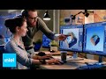 From Sand to Silicon: The Making of a Microchip | Intel
 Introduction to EBL
 Designing 7-nm IP, Bring It On Moore! | Synopsys
 Lecture - 23 Lithography - I
 Learning styles & the importance of critical self-reflection | Tesia Marshik | TEDxUWLaCrosse
 EUV: Lasers, plasma, and the sci-fi tech that will make chips faster | Upscaled
 Jan Vardaman: Semiconductor Packaging and 3D IC: P1
 Nanofabrication Techniques: Photolithography
 2.5 D & 3D Chips: Interposers and Through Silicon Vias
 How semiconductors work