Double Patterning to the rescue (LELE, LFLE, SADP) - Part 1
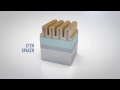
Introduction to Double Patterning which is used extensively for printing transistors and other features in front end of line (FEOL) flow in a semiconductor chip.
This video also introduces the various processing options to achieve double patterning i.e.
1. Litho Etch Litho Etch (LELE)
2. Litho Freeze Litho Etch (LFLE)
3. Self Aligned Double Patterning (SADP)
Видео Double Patterning to the rescue (LELE, LFLE, SADP) - Part 1 канала nanolearning
This video also introduces the various processing options to achieve double patterning i.e.
1. Litho Etch Litho Etch (LELE)
2. Litho Freeze Litho Etch (LFLE)
3. Self Aligned Double Patterning (SADP)
Видео Double Patterning to the rescue (LELE, LFLE, SADP) - Part 1 канала nanolearning
Показать
Комментарии отсутствуют
Информация о видео
Другие видео канала
 Lam Research: Multiple Patterning Enables Feature Shrink (2016)
 Double Patterning to the rescue (Self Aligned Double Patterning) - Part 2
 Understanding The FinFet Semiconductor Process
 Designing 7-nm IP, Bring It On Moore! | Synopsys
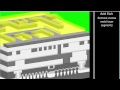 Semitracks: Intel Ivy Bridge 22nm FinFET Process Fabrication
 FinFETs
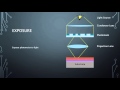 Photolithography: Step by step
 FinFET.wmv
 The Evolution Of CPU Processing Power Part 1: The Mechanics Of A CPU
 Lecture 59 (CHE 323) Lithography Double Patterning
 How a CPU is made
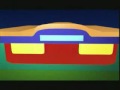 The Fabrication of Integrated Circuits
 Why FinFETs ? Part 1
 DVD - Lecture 10: Packaging and I/O Circuits
 Sam Sivakumar of Intel talks about Lithography and Patterning: Part 1
 CROSSTALK & SHIELDING - English Version
 Self Aligned Contacts (SAC)
 Metallography Part II - Microscopic Techniques
 Front End Of Line : Part 1