How I reverse engineer a chip
A whirlwind tour of my procedure going from physical chip to annotated die image to schematic to wiki page to you!
Some updates since I made this video: I no longer have a Patreon. I ditched them after they started becoming unfriendly to small contributors and small projects by making the fee structure punishing for those.
Also, why do this? For me personally, it's primarily curiosity, a DIY desire to build up skills, my own education, and trying to build a nice library of images on https://project5474.org for others to learn from. There are practical applications for more modern chips, namely investigations for patent infringement, and of course competitive research. "Reverse engineering" doesn't just mean "I don't know how this works", but "I want to find out exactly how this was implemented". Different chip manufacturers built the same logic chips in different ways and it's interesting to see the differences.
More on the process:
* Hot sulfuric acid decapsulation of plastic packages: https://youtu.be/07b6ba5DBtI
* Heat decapsulation of ceramic packages: https://youtu.be/wnQ8Td1y_dM
* Reverse engineering a simple CMOS chip: https://youtu.be/FMdYuGpPicw
Видео How I reverse engineer a chip канала Robert Baruch
Показать
Комментарии отсутствуют
Информация о видео
Другие видео канала
 How Microchips are made
 Intro to Hardware Reversing: Finding a UART and getting a shell
 27c3: Reverse Engineering the MOS 6502 CPU (en)
 Sega Saturn CD - Cracked after 20 years
 How Sega bet against Reverse Engineering...and lost | MVG
 The Missing Link in Renewables
 DEF CON 24 - Hardware Hacking Village - Matt DuHarte - Basic Firmware Extraction
 Electronics Reverse Engineering Walkthrough - Hacking the Monoprice Select Mini 3D Printer
 The Evolution Of CPU Processing Power Part 1: The Mechanics Of A CPU
 Reverse engineering vintage Japanese electronics - a vacuum fluorescent display!
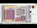 Reverse engineering a simple CMOS chip
 PCB Reverse Engineering
 Decapping ICs (removing epoxy packaging from chips to expose the dies)
 Reverse engineering C programs - bin 0x10
 Simple Tools and Techniques for Reversing a binary - bin 0x06
 learning to reverse engineer routers - reading serial flash ROMs
 Reverse engineering of a mains power controller.
 Oliver Wing - Xbox Firmware Engineer (Prod by GT20)
 Radio Hacking: Cars, Hardware, and more! - Samy Kamkar - AppSec California 2016