- Популярные видео
- Авто
- Видео-блоги
- ДТП, аварии
- Для маленьких
- Еда, напитки
- Животные
- Закон и право
- Знаменитости
- Игры
- Искусство
- Комедии
- Красота, мода
- Кулинария, рецепты
- Люди
- Мото
- Музыка
- Мультфильмы
- Наука, технологии
- Новости
- Образование
- Политика
- Праздники
- Приколы
- Природа
- Происшествия
- Путешествия
- Развлечения
- Ржач
- Семья
- Сериалы
- Спорт
- Стиль жизни
- ТВ передачи
- Танцы
- Технологии
- Товары
- Ужасы
- Фильмы
- Шоу-бизнес
- Юмор
Why is it Called P-Type? | Semiconductor Quick Revision 🔬 #shorts #examprep #physics #semiconductors
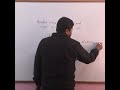
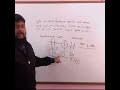
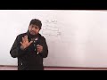
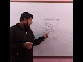
The "P" in P-type doesn't stand for positive charge, but for Positive charge carriers (Holes)! Here’s a rapid revision on how they are manufactured.
Process Explained:
1. Start with Pure (Intrinsic) Semiconductor.
2. Dope it with a Trivalent Impurity (Group 13 element).
3. Each dopant atom creates a "Hole" or Acceptor Level.
4. Holes become the Majority Charge Carriers.
Like & Save this Short for your last-minute Class 12 Electronics revision! Don't forget to check the playlist for full chapter coverage.
#Shorts #Class12 #PhysicsShorts #PtypeSemiconductor #ElectronicsClass12 #HowItsMade #Doping #AcceptorAtom #Holes #BoardExams2025 #StudyWithMe #ShortVideo #education
@phys
@MdSumonHossen @MdSumonHossen @Rizuanaakhtar @ALLENCareerInstituteofficia
@KochuBigganiiiii @StorywiseAcademy @wikifizik @MinutePhysics
@PhysicsYT @Theory_of_Physics @PW-Foundation @Cheenta
@PhysicsYT
@KochuBigganiiiii
Видео Why is it Called P-Type? | Semiconductor Quick Revision 🔬 #shorts #examprep #physics #semiconductors канала Wikifizik Education
Комментарии отсутствуют
Информация о видео
14 января 2026 г. 21:18:52
00:01:45
Другие видео канала