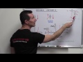
EEVblog #678 - What is a PCB Spark Gap?
In this tutorial Dave explains what a PCB spark gap is and how it can be a useful zero cost addition to your PCB layout to help prevent ESD damage.
He shows how to easily design them into your board and calculate the approximate voltage rating.
And of course has some fun applying 5kV to some gaps to show how them at work.
Plugpack teardown: https://www.youtube.com/watch?v=_EMAggN5H-w
Support the EEVblog through Patreon!
http://www.patreon.com/eevblog
Forum: http://www.eevblog.com/forum/blog/eevblog-678-what-is-a-pcb-spark-gap/
EEVblog Main Web Site: http://www.eevblog.com
The 2nd EEVblog Channel: http://www.youtube.com/EEVblog2
EEVblog Amazon Store (Dave gets a cut):
http://astore.amazon.com/eevblogstore-20
Donations:
http://www.eevblog.com/donations/
Projects:
http://www.eevblog.com/projects/
Electronics Info Wiki:
http://www.eevblog.com/wiki/
Видео EEVblog #678 - What is a PCB Spark Gap? канала EEVblog
Показать
Комментарии отсутствуют
Информация о видео
Другие видео канала
 EEVblog #908 - Zener Diodes
 Making a Spark-Gap Transmitter
 EEVblog #470 - Agilent N9344C 20GHz Spectrum Analyser Teardown
 Evidence for Ancient High Technology - Part 1: Machining
 SDG #078 Creepage and Clearances - Adding mechanical routing to your PCB
 EEVblog #1064 - Soldering Irons OLD vs NEW
 We Rediscover Spark Gap Radio by Accident
 EEVblog #637 - Omni Directional Laser Barcode Scanner Teardown
 EEVblog #1238 - Vion: The World's Worst Multimeter!
 EEVblog #671 - White Van Speaker Scam Teardown
 EEVblog #676 - RANT: FTDI Bricking Counterfeit Chips!
 EEVblog #859 - Bypass Capacitor Tutorial
 EEVblog #532 - Silicon Chip Wafer Fab Mailbag
 EEVblog #994 - CERN/Fermilab Particle Accelerator Boards!
 EEVBlog #1116 - How to Remove Power Supply Ripple
 EEVblog #388 - Fake Apple USB Charger Teardown
 EEVblog #638 - Apollo Saturn V LVDC Testing
 EEVblog #127 - PCB Design For Manufacture Tutorial - Part 1
 EEVblog #600 - OpAmps Tutorial - What is an Operational Amplifier?
 EEVblog #317 - PCB Tinning Myth Busting