Intel Mask Operation: An Inside Look at a Critical Manufacturing Step
Around the corner from Intel’s Santa Clara, California, headquarters is an unassuming building that houses a critically important step in the process of manufacturing chips: the Intel Mask Operation. A mask is a six-by-six-inch piece of quartz, a quarter-inch thick, that’s a template or master copy used to print circuitry onto a silicon wafer. (Credit: Intel Corporation)
More on manufacturing at Intel: https://newsroom.intel.com/press-kits/global-manufacturing/
Видео Intel Mask Operation: An Inside Look at a Critical Manufacturing Step канала Intel Newsroom
More on manufacturing at Intel: https://newsroom.intel.com/press-kits/global-manufacturing/
Видео Intel Mask Operation: An Inside Look at a Critical Manufacturing Step канала Intel Newsroom
Показать
Комментарии отсутствуют
Информация о видео
Другие видео канала
 The Extreme Physics Pushing Moore’s Law to the Next Level
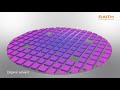 Electron Beam Lithography
 Intel's Fab 42: A Peek Inside One of the World’s Most Advanced Factories
 Maskless Photolithography Stepper for Homemade Chips
 How Intel Makes Chips: Concept to Customer
 A visit to ASML's cleanroom for EUV
 Photomasks Explained (Contact and Projection): how to etch Thin Chromium Layers
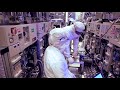 Inside Intel's D1X: The World's Most Advanced Manufacturing Factory
 Zoom Into a Microchip
 Photolithography without a mask: Multilayer lithography with the Maskless Aligner MLA150
 Amazing Biggest plywood woodworking Machine, Fastest Large wood processor Machines Working
 Inside a Huge PCB Factory - in China
 Lam Research: Multiple Patterning Enables Feature Shrink (2016)
 Reticle Shot Map Tutorial
 The Most Sophisticated Manufacturing Process in the World | Inside the Fab | Intel
 Maskless Photolithography with DLP Projector - 10um Feature Sizes
 How Extreme Ultraviolet Lithography works | Part 1/3
 From the ASML archives: "PAS 5500 - The Inside Story" (1993)
 Inside The Worlds Largest Semiconductor Factory - BBC Click