PiN diode - design of the termination region
PiN diode.
Design of the termination region: floating rings and field plates.
Видео PiN diode - design of the termination region канала Power Devices and Circuits
Design of the termination region: floating rings and field plates.
Видео PiN diode - design of the termination region канала Power Devices and Circuits
Показать
Комментарии отсутствуют
Информация о видео
7 ноября 2014 г. 20:04:51
00:48:58
Другие видео канала
 The structure and the IV characteristic of the Silicon Controlled Rectifier (SCR)
 The Forward converter (part2)
 Schottky power diode
 PiN diode. Spice simulation of the reverse recovery
 IV characteristic of the Power MOS
![[ITA] Informazioni riguardanti il corso di Power Devices and Circuits](https://i.ytimg.com/vi/2vA56a3nyb0/default.jpg) [ITA] Informazioni riguardanti il corso di Power Devices and Circuits
[ITA] Informazioni riguardanti il corso di Power Devices and Circuits Introduction
 On state resistance of the Power MOS
 Un ricordo del Prof. Luciano.
 PiN diode - IV characteristic
 The current gain of the Power Bipolar Junction Transistor
 Breakdown voltage for a PN junction
 Thermal instability in Power Bipolar Junction Transistor
 Switching behavior of the Power Bipolar Junction Transistor
 The datasheet of commercial Silicon Controlled Rectifiers (SCR)
 The dynamic behavior of the Silicon Controlled Rectifier (SCR)
 Device power dissipation
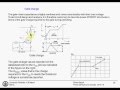 The gate Charge for the Power MOS
 Introduction to Wide Bandgap power semiconductor devices
 GaN Power devices - the HEMT