- Популярные видео
- Авто
- Видео-блоги
- ДТП, аварии
- Для маленьких
- Еда, напитки
- Животные
- Закон и право
- Знаменитости
- Игры
- Искусство
- Комедии
- Красота, мода
- Кулинария, рецепты
- Люди
- Мото
- Музыка
- Мультфильмы
- Наука, технологии
- Новости
- Образование
- Политика
- Праздники
- Приколы
- Природа
- Происшествия
- Путешествия
- Развлечения
- Ржач
- Семья
- Сериалы
- Спорт
- Стиль жизни
- ТВ передачи
- Танцы
- Технологии
- Товары
- Ужасы
- Фильмы
- Шоу-бизнес
- Юмор
PCB ReTrace Demo: Turning traced nets into KiCad Schematics
Overview
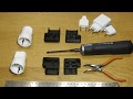
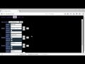
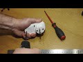
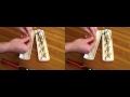
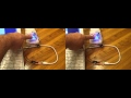
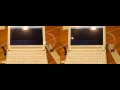
A quick demo of the new "Schema ReTrace" feature in PCB ReTrace, a free, open-source, and entirely browser-based tool for documenting and reverse-engineering printed circuit boards.
In this video, we take a previously traced board (a UPS circuit) and use the new Schema builder to visually arrange the extracted components and nets. We also demonstrate fetching standard KiCad symbol libraries directly in the browser, swapping out generic components for standard schematic symbols, organizing the layout, and exporting the final result as a native KiCad .kicad_sch file.
Everything you see runs 100% locally in your web browser—no cloud uploads required!
🔗 Links:
Try it live: https://pcb.etaras.com/
GitHub Repository: https://github.com/dev-lab/pcb-retrace
Follow the project on Hackaday: https://hackaday.io/project/204738-pcb-retrace
⏱️ Timestamps (Video Chapters):
00:00 - Intro & Loading an Example Board
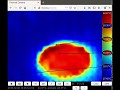
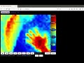
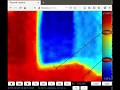
00:15 - Reviewing Traced Data (Images, BOM, and Nets)
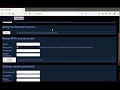
00:21 - Opening the new Schema Builder
00:41 - Fetching & Parsing KiCad Symbol Libraries (In-browser)
01:32 - Replacing Generic Symbols with Standard KiCad Symbols
01:43 - Cross-referencing Component Datasheets
01:54 - Swapping Resistor Symbols
02:15 - Arranging & Rotating the Schematic Layout
02:50 - Exporting and Downloading a KiCad (.kicad_sch) file
Видео PCB ReTrace Demo: Turning traced nets into KiCad Schematics канала Taras Greben
A quick demo of the new "Schema ReTrace" feature in PCB ReTrace, a free, open-source, and entirely browser-based tool for documenting and reverse-engineering printed circuit boards.
In this video, we take a previously traced board (a UPS circuit) and use the new Schema builder to visually arrange the extracted components and nets. We also demonstrate fetching standard KiCad symbol libraries directly in the browser, swapping out generic components for standard schematic symbols, organizing the layout, and exporting the final result as a native KiCad .kicad_sch file.
Everything you see runs 100% locally in your web browser—no cloud uploads required!
🔗 Links:
Try it live: https://pcb.etaras.com/
GitHub Repository: https://github.com/dev-lab/pcb-retrace
Follow the project on Hackaday: https://hackaday.io/project/204738-pcb-retrace
⏱️ Timestamps (Video Chapters):
00:00 - Intro & Loading an Example Board
00:15 - Reviewing Traced Data (Images, BOM, and Nets)
00:21 - Opening the new Schema Builder
00:41 - Fetching & Parsing KiCad Symbol Libraries (In-browser)
01:32 - Replacing Generic Symbols with Standard KiCad Symbols
01:43 - Cross-referencing Component Datasheets
01:54 - Swapping Resistor Symbols
02:15 - Arranging & Rotating the Schematic Layout
02:50 - Exporting and Downloading a KiCad (.kicad_sch) file
Видео PCB ReTrace Demo: Turning traced nets into KiCad Schematics канала Taras Greben
Комментарии отсутствуют
Информация о видео
Вчера, 2:08:19
00:03:17
Другие видео канала