Designing PS3 Cell Frankenstein (Why retrofitting 65 or 45nm Cell BE is difficult)
If somebody wants to continue this project, I have shared all the latest files here - https://www.psx-place.com/threads/90nm-to-65nm-cell-converter-unfinished-project-files.42257/
This example uses COK and SEM boards to outline the differences. SEM board (40gb fat ps3 ) is the first one when Sony made a jump from 90 to 65nm Cell. Keep in mind, while we can directly compare both pinouts by using service manuals, there is no manual for the 45nm revision. However, we can assume the 45nm would be very similar to the 65nm.
Intro 00:00
First challenge - 00:49
Second challenge - 3:43
Third challenge - 5:28
Fourth challenge - 6:38
Why even do it ? - 7:06
Видео Designing PS3 Cell Frankenstein (Why retrofitting 65 or 45nm Cell BE is difficult) канала Calyps0man
Показать
Комментарии отсутствуют
Информация о видео
Другие видео канала
 Repairing unusual fault on a refurbished 65nm PS3 CECHA (Syscon Errors & Explanations)
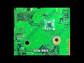 RSX Mod Resistor Corrections and Different Motherboards
 Common PlayStation 2 Disc Scratching Fault Repair
 CECHC vs CECHA PS2 on PS3 Upscaling Comparison
 Designing & Building a BGA Rework Station based on a T8280 (For Frankensteining and more...)
 Reballing stand mod
 Ghetto 3D Printed Smoke Remover
 Reverse Engineering PlayStation 3 Super Slim (Mapping 28nm RSX pads & Interposer research)
 PS3 GPU Swap running without modchip (No more orbis mod needed)
 PlayStation 3 Frankenstein Board versus Orbis Mod (Story and Explanation)
 PS3 Frankenstein - Retrofitting 40nm without Orbis mod (how it's made with explanations )
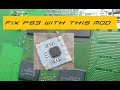 PS3 YLOD repair newest method (RSX Mod)
 Sony Bravia KDL-46EX700 TV Repair
 Upgraded 40nm RSX PS3 Temperature Test (CECHC04/Backwards Compatible)
 How to reball a GPU