- Популярные видео
- Авто
- Видео-блоги
- ДТП, аварии
- Для маленьких
- Еда, напитки
- Животные
- Закон и право
- Знаменитости
- Игры
- Искусство
- Комедии
- Красота, мода
- Кулинария, рецепты
- Люди
- Мото
- Музыка
- Мультфильмы
- Наука, технологии
- Новости
- Образование
- Политика
- Праздники
- Приколы
- Природа
- Происшествия
- Путешествия
- Развлечения
- Ржач
- Семья
- Сериалы
- Спорт
- Стиль жизни
- ТВ передачи
- Танцы
- Технологии
- Товары
- Ужасы
- Фильмы
- Шоу-бизнес
- Юмор
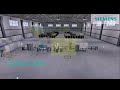
Calibre 3DStress - Chip-package Stress Analysis for 3D IC Designs
Siemens EDA Calibre 3D Stress is transforming how engineers design reliable 3D ICs and chiplets. As part of the Calibre Multiphysics suite, it delivers advanced thermo-mechanical simulation and stress-aware analysis to predict and prevent reliability issues before manufacturing.
In this presentation, Shedda Nolke, Principal Product Manager for Calibre 3D Stress, explains how the solution enables early “what-if” analysis, chip-level optimization, and accurate modeling of mechanical and electrical stress — helping teams achieve robust, high-performance semiconductor designs.
Timestamps
0:00 – Introduction: Shedda Nolke, Siemens EDA
0:10 – Announcing Calibre 3D Stress within Calibre Multiphysics suite
0:31 – Combining chip design and stress simulation for advanced reliability
1:17 – Understanding electrical impacts of stress at transistor level
1:46 – How Calibre 3D Stress fits into Siemens EDA’s 3D IC ecosystem
2:18 – Helping chiplet designers make early, reliability-driven decisions
3:08 – Preventing thermal and mechanical failures during packaging
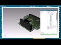
3:37 – Multi-scale simulation and visualization capabilities
4:21 – Parallelization for fast signoff using existing Calibre compute
5:09 – Enabling stress-aware circuit analysis
5:23 – Supported flows and simulation inputs
5:57 – Customer success: STMicroelectronics use case
6:16 – Summary and benefits of Calibre 3D Stress
Discover how Siemens EDA is driving innovation, reliability, and precision in next-generation semiconductor systems.
▶️ Connect with us:
» LinkedIn: https://sie.ag/6FysfA
» Visit our website: https://sie.ag/3h2CKQ
#SiemensEDA #Calibre3DStress #3DIC #ChipletDesign #Semiconductor #Reliability #Innovation #EDA #Technology #Calibre #DesignVerification
Видео Calibre 3DStress - Chip-package Stress Analysis for 3D IC Designs канала Siemens Software
In this presentation, Shedda Nolke, Principal Product Manager for Calibre 3D Stress, explains how the solution enables early “what-if” analysis, chip-level optimization, and accurate modeling of mechanical and electrical stress — helping teams achieve robust, high-performance semiconductor designs.
Timestamps
0:00 – Introduction: Shedda Nolke, Siemens EDA
0:10 – Announcing Calibre 3D Stress within Calibre Multiphysics suite
0:31 – Combining chip design and stress simulation for advanced reliability
1:17 – Understanding electrical impacts of stress at transistor level
1:46 – How Calibre 3D Stress fits into Siemens EDA’s 3D IC ecosystem
2:18 – Helping chiplet designers make early, reliability-driven decisions
3:08 – Preventing thermal and mechanical failures during packaging
3:37 – Multi-scale simulation and visualization capabilities
4:21 – Parallelization for fast signoff using existing Calibre compute
5:09 – Enabling stress-aware circuit analysis
5:23 – Supported flows and simulation inputs
5:57 – Customer success: STMicroelectronics use case
6:16 – Summary and benefits of Calibre 3D Stress
Discover how Siemens EDA is driving innovation, reliability, and precision in next-generation semiconductor systems.
▶️ Connect with us:
» LinkedIn: https://sie.ag/6FysfA
» Visit our website: https://sie.ag/3h2CKQ
#SiemensEDA #Calibre3DStress #3DIC #ChipletDesign #Semiconductor #Reliability #Innovation #EDA #Technology #Calibre #DesignVerification
Видео Calibre 3DStress - Chip-package Stress Analysis for 3D IC Designs канала Siemens Software
Комментарии отсутствуют
Информация о видео
15 ноября 2025 г. 20:01:51
00:07:08
Другие видео канала