- Популярные видео
- Авто
- Видео-блоги
- ДТП, аварии
- Для маленьких
- Еда, напитки
- Животные
- Закон и право
- Знаменитости
- Игры
- Искусство
- Комедии
- Красота, мода
- Кулинария, рецепты
- Люди
- Мото
- Музыка
- Мультфильмы
- Наука, технологии
- Новости
- Образование
- Политика
- Праздники
- Приколы
- Природа
- Происшествия
- Путешествия
- Развлечения
- Ржач
- Семья
- Сериалы
- Спорт
- Стиль жизни
- ТВ передачи
- Танцы
- Технологии
- Товары
- Ужасы
- Фильмы
- Шоу-бизнес
- Юмор
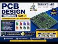
PCB Design Training Day 13 (Part 1) | EMI & EMC Basics | Noise Reduction in PCB Design
Welcome to Day 13 (Part 1) of PCB Design Training by SURYA’S MiB Enterprises! ⚡
In this session, we begin with EMI (Electromagnetic Interference) and EMC (Electromagnetic Compatibility) — very important concepts for industrial and high-performance PCB design.
🔍 What you will learn in this video:
What is EMI and EMC in PCB design
Sources of noise in electronic circuits
Effects of electromagnetic interference
Basics of shielding and grounding
Importance of proper PCB layout for noise reduction
Real-world examples of EMI issues
This session builds the foundation for designing stable, noise-free, and industry-standard PCBs.
🎯 Who should watch:
Advanced PCB learners
Electronics & Embedded students
Hardware design engineers
🎓 Career Benefit:
Understanding EMI/EMC helps you design professional-grade PCBs used in real-world electronic products.
📢 Training & Certification:
Enroll in our PCB Design Training with real-time industry concepts.
📞 Contact: SURYA’S MiB – 8124227370
🚀 Stay tuned for Day 13 (Part 2) where we will cover EMI/EMC design techniques and practical implementation!
#PCBDesign #PCBTutorial #PCBDesignTraining #CircuitDesign #ElectronicsDesign #PCBLayout #PrintedCircuitBoard #PCBDesigner #AltiumDesigner #KiCad #EaglePCB #OrCAD #Proteus #CadencePCB #EasyEDA #LearnPCB #ElectronicsEngineering #EngineeringStudents #OnlineLearning #TechTraining #SkillDevelopment #PCBClass #Tech #Engineering #DIYElectronics #ElectronicsProjects #Innovation #STEM #TechEducation
Видео PCB Design Training Day 13 (Part 1) | EMI & EMC Basics | Noise Reduction in PCB Design канала SURYA'S MiB
Комментарии отсутствуют
Информация о видео
13 мая 2026 г. 6:30:06
00:16:26
Другие видео канала