Intentionally Shattering Wafers | Inside the Fab | Intel
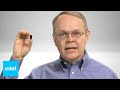
Meet Ryan Parrott, Packaging Engineer at Intel. His job is to design and test the custom packaging solutions used to ship silicon wafers all over the world. In order to learn which solutions work, Ryan has got to push expensive wafers potentially containing thousands of processors to their breaking points.
The packaging used to ship wafers is called a Front-Opening Shipping Box, or FOSB. Each of these specially-designed boxes contain 25 glass-like, silicon wafers totaling $250,000 to multi-million US dollars per box depending on product. Each wafer is incredibly fragile, and it's Ryan's job to insure that each FOSB makes it to its destination with all wafers intact.
Check out Ryan's story, and stay tuned for more stories "Inside the Fab" at Intel. Subscribe now to Intel on YouTube: http://bit.ly/1BZDtpf
About Intel:
Intel, the world leader in silicon innovation, develops technologies, products and initiatives to continually advance how people work and live. Founded in 1968 to build semiconductor memory products, Intel introduced the world's first microprocessor in 1971. This decade, our mission is to create and extend computing technology to connect and enrich the lives of every person on earth.
Connect with Intel:
Visit Intel WEBSITE: http://intel.ly/1WXmVMe
Like Intel on FACEBOOK: http://intel.ly/1wrbYGi
Follow Intel on TWITTER: http://intel.ly/1wrbXC8
Follow Intel on INSTAGRAM: http://bit.ly/1OJuPTg
Intentionally Shattering Wafers | Inside the Fab | Intel
https://www.youtube.com/user/channelintel
Видео Intentionally Shattering Wafers | Inside the Fab | Intel канала Intel
Показать
Комментарии отсутствуют
Информация о видео
Другие видео канала
 The Most Sophisticated Manufacturing Process in the World | Inside the Fab | Intel
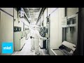 Working in the Clean Room | Inside the Fab | Intel
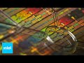 Silicon Manufacturing & The Perfect Wafer | Inside the Fab | Intel
 From Sand to Silicon: The Making of a Microchip | Intel
 Video Animation: Mark Bohr Gets Small: 22nm Explained | Intel
 A Day in the Life of Otis: An Intel Manufacturing Technician | Intel
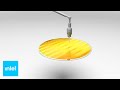 From Sand to Silicon: the Making of a Chip | Intel
 Puzzle Pieces the Size of Houses | Inside the Fab | Intel
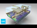 Sand to Silicon - the Making of a Chip (full screen) | Intel
 Moore's Law Got Me! | Intel
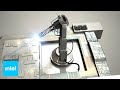 The Power of Small - 3rd Generation Intel® Core™ | Intel
 The Robotic Musicians known as: Intel's Industrial Control in Concert | Intel
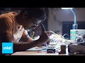 Shubham Banerjee & Intel Edison | Meet the Makers | Intel
 Intel: The Making of a Chip with 22nm/3D Transistors | Intel
 64-bit Mobile Computing Animation | Intel
 Processor Installation in a LGA1150 Socket | Intel
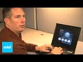 Turbo Mode inside Intel's Core i7 | Intel
 SSD vs. HDD with Intel SSDs | Intel
 Intel's Experience Vision | Intel