Transmission du signal vidéo entre carte mère et carte Tcon via le LVDS. La norme VESA et JEIDA
Cette vidéo aborde plusieurs notions dont le standard VESA et JEIDA. Le cheminement du signal vidéo via le système LVDS et sa transmission depuis la carte mère du téléviseur jusqu’à l’afficheur LCD en transitant par la carte TCON. La notion de convertisseur de data parallèle à série connu aussi sous le nom de serializer déserializer.
Видео Transmission du signal vidéo entre carte mère et carte Tcon via le LVDS. La norme VESA et JEIDA канала e-learning électronique
Видео Transmission du signal vidéo entre carte mère et carte Tcon via le LVDS. La norme VESA et JEIDA канала e-learning électronique
Показать
Комментарии отсутствуют
Информация о видео
Другие видео канала
 Signs of LCD TV screen defect Horizontal line, double image and screen breakage
 Identification and function of the T Con board in an LCD TV
 Internal structure of a liquid crystal or LCD TV screen
 VGH and VGL production mode by the TCON board. The charge pump converter.
 VDD and AVVD voltage production mode by the TCON board . The Buck and boost converters.
 Video signal transmission between motherboard and Tcon via LVDS. VESA and JEIDA standard
 Meaning of the LVDS used between the motherboard of an LCD TV and the TCON board
 The Gamma chip of the TCON board and the role of the opamp configured as a voltage follower
 Role of the Gamma chip of the TCON board in an LCD TV
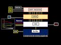 Meaning of STH CPH TP POL SOE STB and relationship between TCON Gamma and source driver
 Signification de STH CPH TP POL SOE STB et relation entre le Gamma du TCON avec le source driver
 What does it mean on a TCON board CPV CKV CKVB STV STVP OE XAO RL UD VGH VGL
 Que signifie sur une carte TCON les termes CPV CKV CKVB STV STVP OE XAO RL UD VGH VGL
 Geometry of pixels in an LCD screen and their control by the Gate driver
 Géométrie des Pixels dans un écran LCD et modalité de leur contrôle par le pilote de grille
 Organization of the pixels in LCD screen and the different circuits of their control from the TCON
 Organisation des pixels dans un écran LCD et les différents circuits de leur commande depuis le TCON
 Signification du LVDS utilisé entre la carte mère d'une TV LCD et la carte TCON
 La puce Gamma de la carte T CON Rôle de l'AOP suiveur de tension
 Rôle de la puce Gamma de la carte TCON dans un téléviseur LCD