
- Популярные видео
- Авто
- Видео-блоги
- ДТП, аварии
- Для маленьких
- Еда, напитки
- Животные
- Закон и право
- Знаменитости
- Игры
- Искусство
- Комедии
- Красота, мода
- Кулинария, рецепты
- Люди
- Мото
- Музыка
- Мультфильмы
- Наука, технологии
- Новости
- Образование
- Политика
- Праздники
- Приколы
- Природа
- Происшествия
- Путешествия
- Развлечения
- Ржач
- Семья
- Сериалы
- Спорт
- Стиль жизни
- ТВ передачи
- Танцы
- Технологии
- Товары
- Ужасы
- Фильмы
- Шоу-бизнес
- Юмор
MOSFET Biasing, Transconductance and Small Signal Model Explained
An nMOS (n-channel MOSFET) is a voltage-controlled device with four terminals: gate (G), drain (D), source (S), and body/bulk (B). In most circuits the body is tied to the source, so it behaves like a three-terminal part. With a DC bias, it operates in three regions set by the gate-source overdrive (VGS − VT): cutoff , triode/linear, and saturation/active ( acts like a current source). Designers usually bias in saturation for amplification. Channel-length modulation means the effective channel shortens as VDS increases, so the drain current still rises slightly in saturation, giving the device a finite output resistance. If the body isn’t tied to the source, the body effect raises VT as VSB increases.
For small-signal analysis around a chosen bias point, replace the device with its hybrid-pi model: the gate is effectively open (very high input resistance), the drain is represented by a current source controlled by vgs with transconductance gm, and an output resistance ro is placed from drain to source to model channel-length modulation. If the body isn’t at the source, include a second, smaller transconductance gmb controlled by vbs. Typical workflow: pick a bias so the device stays in saturation, determine gm and ro from that bias (or from datasheet/model), then use the small-signal model to compute gain, input/output resistances, and bandwidth in the surrounding circuit (e.g., a common-source stage has negative voltage gain roughly set by gm and the load seen at the drain).
00:00 n-MOS basics
4:46 Biasing
6:03 Transconductance
8:29 Channel length modulation
11:15 Small Signal Model
Видео MOSFET Biasing, Transconductance and Small Signal Model Explained канала YS Electronics
For small-signal analysis around a chosen bias point, replace the device with its hybrid-pi model: the gate is effectively open (very high input resistance), the drain is represented by a current source controlled by vgs with transconductance gm, and an output resistance ro is placed from drain to source to model channel-length modulation. If the body isn’t at the source, include a second, smaller transconductance gmb controlled by vbs. Typical workflow: pick a bias so the device stays in saturation, determine gm and ro from that bias (or from datasheet/model), then use the small-signal model to compute gain, input/output resistances, and bandwidth in the surrounding circuit (e.g., a common-source stage has negative voltage gain roughly set by gm and the load seen at the drain).
00:00 n-MOS basics
4:46 Biasing
6:03 Transconductance
8:29 Channel length modulation
11:15 Small Signal Model
Видео MOSFET Biasing, Transconductance and Small Signal Model Explained канала YS Electronics
Комментарии отсутствуют
Информация о видео
31 августа 2025 г. 16:00:51
00:15:57
Другие видео канала
 How to Solve Inverting Op-Amp Exercises (Summing Amplifier, Grounded Resistor)
 How to Solve MOSFET circuits, Diode connected (EXAM topic, Channel Length Modulation)
 Golden Rules of the Op-Amp explained in less than 5 minutes
 How to Solve Inverting Op-Amp Exercises (Close loop gain)
 How to Solve 2 Op-Amp Exercises (Floating Output)
 How to Solve Inverting Op-Amps with Capacitors (Transfer function behavior)
 How to Solve Diode Circuits, Draw Output Diagram for input Sine
 MOSFET Common Source Amplifier Explained
 How to Solve Diode Circuits (2 diodes, 4 cases)
 Operational Amplifiers: Op-Amp Integrator Analyzed (With Solved Example)
 Operational Amplifiers: Op-Amp as Differential Amplifier or Op-Amp as subtractor (With Example)
 How to Solve Inverting Op-Amp Exercises (Multiple Feedback Resistors)
 Diodes in Circuits, Basics of the Constant Voltage Model in 5 minutes
 How to Solve Inverting Op-Amp Exercises| Explained with steps
 Op-Amp: Inverting Summing Amplifier (with Example)
 How to Solve MOSFET circuits (with and without Channel Length Modulation)
 How to Solve p-mos MOSFET circuits (with and without channel length modulation)
 How to Solve 2 Op-Amp Exercises (Two terminal input, find current)
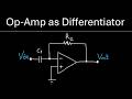 Operational Amplifiers: Op-Amp as Differentiator Analysis (with Example)
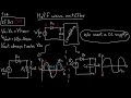 Half Wave Rectifier Analyzed (with capacitor)
