IBM’s Incredible TrueNorth Chip || Neuromorphic Computing
With around 86 billion neurons and up to 1 quadrillion synapse connections, the human brain contains over 400,000 km of nerve fiber; long enough to reach the moon!
All of these connections allow the brain to fire a quintillion calculations per second or one ExaFLOP in Computing Terms.
For the uninitiated, an ExaFLOP is far beyond what the most powerful supercomputer in the world is capable of.
This is the IBM designed OLCF-4, AKA Summit, the fastest supercomputer in the world.
Summit’s speed is generated by 250 refrigerator-sized cabinets taking up over 520 square meters and weighing 340 tons.
With over 200,000 processor cores and over 27,000 GPUs, Summit is capable of 200 quadrillion calculations per second, or 200 petaflops.
That is over 600,000 times faster than the CPU in an iPhone X!
Even with all of Summit’s brut power, the human brain can still make calculations five times faster.
And crazy as it sounds, the next comparison is far more fascinating.
Summit’s over 73 trillion transistors generate so much heat that it requires over 15,000 liters of water a minute, to keep it cool.
The system as a whole consumes 13 MW of power, enough for 13,000 microwaves.
The human brain, on the other hand, consumes just 20 watts of power, less than a single lightbulb!
DRAMATIC PAUSE
Why are computers far superior to humans at performing specific specialized tasks but do not come close to humans regarding cognitive faculties like perception, imagination, and consciousness?
And how does the brain have five times the flops as Summit while being 130,000 times more efficient?
While there are many answers to these questions, the differences boil down to architecture.
Today’s computers are extraordinarily complex, yet they are based on the Von Neumann Architecture dating back to 1945!
This architecture has four components:
First is the Control Unit that decodes instructions and controls how the data flows through the computer.
Second is the Arithmetic Logic Unit or ALU that processes all of the mathematical operations. The ALU and control unit together make up the Central Processing Unit or CPU.
The third component is the Main Memory Unit, which holds data and instructions.
And fourth is the Input/Output devices.
One of the issues with this architecture is the Von Neumann Bottleneck caused by the separation of memory and processing components.
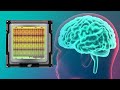
This brings us to IBM’s TrueNorth Chip inspired by the brain.
TrueNorth is the product of 16 years of research from scientists at IBM in Almaden CA led by Dr. Dharmendra Modha.
IBM received DARPA contract in 2008 to develop a new kind of cognitive computer with architecture similar to the brain.
By 2011, IBM built two prototype chips called Golden Gate and San Francisco each containing just 256 neurons, roughly the size of the nervous system of a worm.
Despite the limited number of neurons, the chips were capable of simple cognitive exercises such as playing pong and recognizing handwritten digits.
By 2013, Modha’s team then shrunk the components of the Golden Gate chip by 15-fold and reduced the power consumption by 100-fold to create a neurosynaptic core.
4,096 of these smaller more efficient cores fit together on a 64 x 64 gird forming the TrueNorth Chip equipped with 1 million neurons and 256 million synapses.
The cores operate independently and in parallel with one another.
Each core houses both memory and processing functions as all of the instructions and information needed are store locally and mimics neurons of the brain.
This small section lies the axon buffers containing 256 inputs that receive data spikes like neuron dendrites in the brain.
The Neuron Block holds the 256 neurons which are individually programmed to send its output when its threshold is reached similar to neurons in the brain.
Like the brain, the output are messages called spikes and indicate neuron activity.
The output is sent to the routing network which sends the data to other neurons similar to axon terminals in the brain.
Indeed, the TrueNorth mimics the brains architecture quite well, and it also mimics its efficiency.
With 5.4 billion transistors, TrueNorth is the second largest chip IBM has ever produced and yet it consumes just 73 milliwatts which is around a thousand times less than a typical CPU.
It can run at full blast on an iPhone battery for a whole week.
On top of all of this, TrueNorth can be tiled with other TrueNorth Chips for increasingly complex tasks.
This is the NS16e circuit board incorporating 16 IBM TrueNorth chips.
Since its inception, TrueNorth has proven to be incredibly proficient at machine learning applications such as image recognition.
TrueNorth is capable of monitoring dozens of TV video feeds at the same time and classifies 6,000 images per watt.
To put this in perspective, NVIDA’s Tesla P4 GPU classifies about 160 images per watt.
Видео IBM’s Incredible TrueNorth Chip || Neuromorphic Computing канала NeoScribe
All of these connections allow the brain to fire a quintillion calculations per second or one ExaFLOP in Computing Terms.
For the uninitiated, an ExaFLOP is far beyond what the most powerful supercomputer in the world is capable of.
This is the IBM designed OLCF-4, AKA Summit, the fastest supercomputer in the world.
Summit’s speed is generated by 250 refrigerator-sized cabinets taking up over 520 square meters and weighing 340 tons.
With over 200,000 processor cores and over 27,000 GPUs, Summit is capable of 200 quadrillion calculations per second, or 200 petaflops.
That is over 600,000 times faster than the CPU in an iPhone X!
Even with all of Summit’s brut power, the human brain can still make calculations five times faster.
And crazy as it sounds, the next comparison is far more fascinating.
Summit’s over 73 trillion transistors generate so much heat that it requires over 15,000 liters of water a minute, to keep it cool.
The system as a whole consumes 13 MW of power, enough for 13,000 microwaves.
The human brain, on the other hand, consumes just 20 watts of power, less than a single lightbulb!
DRAMATIC PAUSE
Why are computers far superior to humans at performing specific specialized tasks but do not come close to humans regarding cognitive faculties like perception, imagination, and consciousness?
And how does the brain have five times the flops as Summit while being 130,000 times more efficient?
While there are many answers to these questions, the differences boil down to architecture.
Today’s computers are extraordinarily complex, yet they are based on the Von Neumann Architecture dating back to 1945!
This architecture has four components:
First is the Control Unit that decodes instructions and controls how the data flows through the computer.
Second is the Arithmetic Logic Unit or ALU that processes all of the mathematical operations. The ALU and control unit together make up the Central Processing Unit or CPU.
The third component is the Main Memory Unit, which holds data and instructions.
And fourth is the Input/Output devices.
One of the issues with this architecture is the Von Neumann Bottleneck caused by the separation of memory and processing components.
This brings us to IBM’s TrueNorth Chip inspired by the brain.
TrueNorth is the product of 16 years of research from scientists at IBM in Almaden CA led by Dr. Dharmendra Modha.
IBM received DARPA contract in 2008 to develop a new kind of cognitive computer with architecture similar to the brain.
By 2011, IBM built two prototype chips called Golden Gate and San Francisco each containing just 256 neurons, roughly the size of the nervous system of a worm.
Despite the limited number of neurons, the chips were capable of simple cognitive exercises such as playing pong and recognizing handwritten digits.
By 2013, Modha’s team then shrunk the components of the Golden Gate chip by 15-fold and reduced the power consumption by 100-fold to create a neurosynaptic core.
4,096 of these smaller more efficient cores fit together on a 64 x 64 gird forming the TrueNorth Chip equipped with 1 million neurons and 256 million synapses.
The cores operate independently and in parallel with one another.
Each core houses both memory and processing functions as all of the instructions and information needed are store locally and mimics neurons of the brain.
This small section lies the axon buffers containing 256 inputs that receive data spikes like neuron dendrites in the brain.
The Neuron Block holds the 256 neurons which are individually programmed to send its output when its threshold is reached similar to neurons in the brain.
Like the brain, the output are messages called spikes and indicate neuron activity.
The output is sent to the routing network which sends the data to other neurons similar to axon terminals in the brain.
Indeed, the TrueNorth mimics the brains architecture quite well, and it also mimics its efficiency.
With 5.4 billion transistors, TrueNorth is the second largest chip IBM has ever produced and yet it consumes just 73 milliwatts which is around a thousand times less than a typical CPU.
It can run at full blast on an iPhone battery for a whole week.
On top of all of this, TrueNorth can be tiled with other TrueNorth Chips for increasingly complex tasks.
This is the NS16e circuit board incorporating 16 IBM TrueNorth chips.
Since its inception, TrueNorth has proven to be incredibly proficient at machine learning applications such as image recognition.
TrueNorth is capable of monitoring dozens of TV video feeds at the same time and classifies 6,000 images per watt.
To put this in perspective, NVIDA’s Tesla P4 GPU classifies about 160 images per watt.
Видео IBM’s Incredible TrueNorth Chip || Neuromorphic Computing канала NeoScribe
Показать
Комментарии отсутствуют
Информация о видео
Другие видео канала
 Neuromorphic: BRAINLIKE Computers
 Quantum Computers Explained – Limits of Human Technology
 The TrueNorth Journey: 2008 - 2018
 Brain-Like (Neuromorphic) Computing - Computerphile
 Is 3D STACKING coming sooner than we think?
 Neuromorphic computing with emerging memory devices
 J. Grollier - Neuromorphic computing: overview and challenges
 How to Wire a Computer Like a Human Brain
 How Brain Computing Works (What Is Cognitive Computing)
 Building a Computer Like Your Brain
 There's Plenty Moore Room: IBM's New 2nm CPU
 What Skyscrapers Say About A City's Culture || The US vs Europe vs The Middle East vs Asia
 CPU? GPU? This new ARM chip is BOTH
 Mike Davies: Realizing the Promise of Spiking Neuromorphic Hardware
 Neuromorphic Computing, AI Chips Emulating the Brain with Kelsey Scharnhorst on MIND & MACHINE
 IBM Reveals FIRST 2 Nanometer Chip Tech! (Watch the trailer here)
 The Most Powerful Supercomputer
 TrueNorth Part 1 Explanation Video
 Photonic Neuromorphic Computing: The Future of AI?