- Популярные видео
- Авто
- Видео-блоги
- ДТП, аварии
- Для маленьких
- Еда, напитки
- Животные
- Закон и право
- Знаменитости
- Игры
- Искусство
- Комедии
- Красота, мода
- Кулинария, рецепты
- Люди
- Мото
- Музыка
- Мультфильмы
- Наука, технологии
- Новости
- Образование
- Политика
- Праздники
- Приколы
- Природа
- Происшествия
- Путешествия
- Развлечения
- Ржач
- Семья
- Сериалы
- Спорт
- Стиль жизни
- ТВ передачи
- Танцы
- Технологии
- Товары
- Ужасы
- Фильмы
- Шоу-бизнес
- Юмор
VHDL Part 1: HALF ADDER Design & EDA Playground Setup Explained
Are you ready to level up from basic logic gates to actual binary arithmetic? 🚀 Welcome to the next step in our ultimate VHDL series! In this video, we tackle our very first combinational circuit: The Half Adder.
Because this is a major milestone, we are breaking it down! In Part 1, we focus strictly on the foundation. We walk through setting up your EDA Playground environment and writing the Design file (design.vhd). A Half Adder takes two single-bit binary inputs to generate both a "Sum" and a "Carry" output. You will learn exactly how to combine the XOR and AND logic we covered in previous videos into a single, multi-output VHDL architecture!
⏩ Next Up:
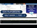
Half Adder Part 2 (Testbench & EP Waveform):
⏪ Need a refresher? Check out the prerequisite VHDL tutorials here:
1) How To Use EDA Playground From Start To Finish (Full Guide): https://youtu.be/WWlwIth4E14?si=7JpBHENInnyCK97Q
2) The Ultimate Guide to EDA Playground: From Zero to Hero (VHDL & Verilog): https://youtu.be/oqgePe5ijgI?si=ZgCqKwS0D4StPbar
3) VHDL Part 1: AND GATE (Two Input) Design & EDA Playground Setup Explained: https://youtu.be/42x_CB6CiO4?si=k6RJ4h4Ldwruf6yV
4) VHDL Part 2: AND Gate (Two Input) Testbench & EP Wave (Output) Explained: https://youtu.be/ko0Vp4l2CWY?si=Lyh8h-vZkr3ADETD
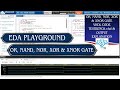
5) VHDL: OR, NAND, NOR, XOR & XNOR Gate (Two Input) Design, Testbench & EP Wave (Output) Explained: https://youtu.be/OdVPTDGikWc?si=MW1H7oBOSaX2kK6r
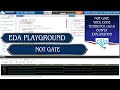
6) VHDL: NOT Gate Design, Testbench & EP Wave (Output) Explained: https://youtu.be/qzpHTsO7mmM?si=mQnnbQPQQcEeoLxt
7) VHDL Part 1: HALF ADDER Design & EDA Playground Setup Explained: https://youtu.be/WzV9RGm37NQ?si=C-alL-n29NS55f6S
Whether you are building your first calculator project or studying for a VLSI exam, this step-by-step breakdown makes combinational logic crystal clear!
⏰ Video Timestamps:
0:00 - Introduction The Half Adder
5:35 - Setting up EDA Playground for Combinational Logic
7:58 - Writing & Explaining the Design Code (design.vhd)
🎓 What You Will Learn:
✅ The fundamental truth table and logic behavior of a Half Adder.
✅ How to set up your EDA Playground workspace for a new project.
✅ How to declare and map multiple outputs (Sum and Carry) within a single VHDL entity.
✅ How to implement concurrent logic statements inside the architecture block.
💝 CONNECT WITH ME:
🔗 LinkedIn: linkedin.com/in/saikat-munshib-3b32b0299
📸 Instagram: instagram.com/techiepapa_sm
📢 Support the Channel!
If this step-by-step tutorial helped you master the design of a Half Adder, please LIKE, SHARE, and SUBSCRIBE to Techie Papa!
💬 Drop any doubts or suggestions in the comments — I reply to everyone!
#VHDL #HalfAdder #DigitalDesign #EDAPlayground #BinaryArithmetic #VLSI #Engineering #Electronics #Coding #TechiePapa #ECE #ComputerScience
Видео VHDL Part 1: HALF ADDER Design & EDA Playground Setup Explained канала Techie Papa
Because this is a major milestone, we are breaking it down! In Part 1, we focus strictly on the foundation. We walk through setting up your EDA Playground environment and writing the Design file (design.vhd). A Half Adder takes two single-bit binary inputs to generate both a "Sum" and a "Carry" output. You will learn exactly how to combine the XOR and AND logic we covered in previous videos into a single, multi-output VHDL architecture!
⏩ Next Up:
Half Adder Part 2 (Testbench & EP Waveform):
⏪ Need a refresher? Check out the prerequisite VHDL tutorials here:
1) How To Use EDA Playground From Start To Finish (Full Guide): https://youtu.be/WWlwIth4E14?si=7JpBHENInnyCK97Q
2) The Ultimate Guide to EDA Playground: From Zero to Hero (VHDL & Verilog): https://youtu.be/oqgePe5ijgI?si=ZgCqKwS0D4StPbar
3) VHDL Part 1: AND GATE (Two Input) Design & EDA Playground Setup Explained: https://youtu.be/42x_CB6CiO4?si=k6RJ4h4Ldwruf6yV
4) VHDL Part 2: AND Gate (Two Input) Testbench & EP Wave (Output) Explained: https://youtu.be/ko0Vp4l2CWY?si=Lyh8h-vZkr3ADETD
5) VHDL: OR, NAND, NOR, XOR & XNOR Gate (Two Input) Design, Testbench & EP Wave (Output) Explained: https://youtu.be/OdVPTDGikWc?si=MW1H7oBOSaX2kK6r
6) VHDL: NOT Gate Design, Testbench & EP Wave (Output) Explained: https://youtu.be/qzpHTsO7mmM?si=mQnnbQPQQcEeoLxt
7) VHDL Part 1: HALF ADDER Design & EDA Playground Setup Explained: https://youtu.be/WzV9RGm37NQ?si=C-alL-n29NS55f6S
Whether you are building your first calculator project or studying for a VLSI exam, this step-by-step breakdown makes combinational logic crystal clear!
⏰ Video Timestamps:
0:00 - Introduction The Half Adder
5:35 - Setting up EDA Playground for Combinational Logic
7:58 - Writing & Explaining the Design Code (design.vhd)
🎓 What You Will Learn:
✅ The fundamental truth table and logic behavior of a Half Adder.
✅ How to set up your EDA Playground workspace for a new project.
✅ How to declare and map multiple outputs (Sum and Carry) within a single VHDL entity.
✅ How to implement concurrent logic statements inside the architecture block.
💝 CONNECT WITH ME:
🔗 LinkedIn: linkedin.com/in/saikat-munshib-3b32b0299
📸 Instagram: instagram.com/techiepapa_sm
📢 Support the Channel!
If this step-by-step tutorial helped you master the design of a Half Adder, please LIKE, SHARE, and SUBSCRIBE to Techie Papa!
💬 Drop any doubts or suggestions in the comments — I reply to everyone!
#VHDL #HalfAdder #DigitalDesign #EDAPlayground #BinaryArithmetic #VLSI #Engineering #Electronics #Coding #TechiePapa #ECE #ComputerScience
Видео VHDL Part 1: HALF ADDER Design & EDA Playground Setup Explained канала Techie Papa
half adder eda playground half adder vhdl vhdl verilog and gate eda half adder eda half adder eda playground vhdl basics how to design and get sum & carry for half adder how to design and get sum & carry for half adder in eda playground and vhdl and eda half half vhdl adder eda half adder in eda playground half adder using eda playground half adder in vhdl half adder using vhdl
Комментарии отсутствуют
Информация о видео
15 мая 2026 г. 15:55:10
00:18:58
Другие видео канала