Howto repair switch mode power supplies #2: Stand-by circuit and its functionality
In the second video in the series of repairing switch mode power supplies (SMPSs) we look at the importance and the functionality of the so called Stand-by circuit. Namely, the low power Stand-by circuit is responsible for generating the Stand-by voltage, which should be always generated by the power s
upply unit (PSU) as soon as your device is plugged into the power grid. This is because the stand-by
voltage is feeding those circuits (most of the time microcontrollers) which are checking the state of
your device and they are waiting for a turn-ON signal. After a microcontroller receives the turn-ON
signal, again the stand-by power is used to send the wake-up signal to the high power portion of the
Switch Mode Power Supply.
Therefore, whenever you try to repair a switch mode PSU, firs you have to make sure, that the Stand-by power section of the PSU is working properly, and it is providing the right voltages to the stand-by circuit. This is because if there is no stand-by power, the device will never able to turn on.
The Stand-by circuit it mostly formed by a small transformer, a medium-power FET transistor and an in
tegrated circuit, which is controlling the gate electrode of the FET.
Thus, if you are able to spot a small transformer on the printed circuit board of your switch mode PSU you are trying to repair, you can be almost sure that it is the stand-by transformer.
In this video I introduce the notion of pulse width modulation (PWM), but this is the most important
topic for switch mode PSUs, so I will cover it in the follow-up video.
Видео Howto repair switch mode power supplies #2: Stand-by circuit and its functionality канала Donkey Learning IT
Показать
Комментарии отсутствуют
Информация о видео
Другие видео канала
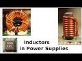 Howto repair switch mode power supplies #3: Inductor in electronic circuits P1
 SMPS repair series #10: Temperature compensated Zener diode in linear regulators
 Como funcionam as fontes chaveadas ATX, Ótima explicação!!!
 Asus Laptop No power Not Charging Repair- How Mosfets work and short circuit diagnosis
 電源供應器-維修DIY-Power supply repair
 #213 Repair Computer Power Supply /ATX Standby Voltage Fail Part 2
 12V Power Supply Repair
 Howto repair switch mode power supplies #1: basics, and block diagram of a PSU
 Power Supply Troubleshooting and Repair Tips
 Howto repair switch mode power supplies #6: Basics of Linear Regulators and voltage references
 #223 How to Design SMPS Switch Mode Power Supply
 Switch Mode Power Supply Repair, SMPS
 How Does a Switching Power Supply Work 1 (schematic, explanation, example, modifications)
 SMPS Switching switch Mode Power Supply repair Basics & Troubleshooting Haseeb Electronics
 How SMPS works | What Components We Need? Switched Mode Power Supply
 How Does a Switching Power Supply Work 2 (measurements)
 Board Repair Basics #10 - Short Detection with Voltage Injection
 Fixing LCD flat screen TV Not turning on No standby LED pt1
 LG LED TV Repair, No power troubleshooting (Tagalog)