300-mm Fab for Thin Silicon Wafer in Villach | Infineon
'Starting in 2011 Infineon Technologies AG has produced the first chips on a 300-millimeter thin silicon wafer for power semiconductors at the Villach site in Austria. This makes Infineon the first company in the world to succeed in taking this step forward.
The chips produced on a 300-millimeter thin wafer exhibit the same behavior as the power semiconductors made on 200-mm silicon wafers – as has been demonstrated by successful application tests using Metal Oxide Semiconductor Field-Effect Transistors (MOSFETs) for High Voltage applications.
Watch our video and see how Infineon has realized a fully automated 300-mm fab for thin silicon wafer in Villach. A milestone in the history of European industry.
Find more information about 300-mm thin silicon wafer technology for power semiconductors: https://www.infineon.com/cms/en/about-infineon/press/press-releases/2011/INFXX201110-002.html
____________
Like this video? Subscribe to Infineon Technologies AG on YouTube: https://www.youtube.com/channel/UCoTflChMPX0VBFXvXYmcu9w?sub_confirmation=1
Infineon Technologies AG is a world leader in semiconductor solutions that make life easier, safer and greener. Microelectronics from Infineon is the key to a better future.
Connect with us on:
Twitter: https://twitter.com/Infineon
Facebook: https://www.facebook.com/Infineon
LinkedIn: https://www.linkedin.com/company/infineon-technologies
#wafertechnology #infineonwafer #waferchips #semiconductorwafer
Видео 300-mm Fab for Thin Silicon Wafer in Villach | Infineon канала Infineon Technologies AG
Показать
Комментарии отсутствуют
Информация о видео
Другие видео канала
 Insight to our new fab in Villach | Infineon
 Siltronic insights
 Why making chips is so hard
 KUKA Cobots at Infineon: The new way of producing semiconductors in cleanroom environments
 "Masterpiece of Construction" - New Factory in Villach | Infineon
 반도체 실리콘 웨이퍼(Wafer) 공정 소개 영상 (KOR)
 Infineon's Facility in Kulim, Malaysia
 #DiscoverInfineon Hydrogen
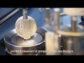 Semiconductor Wafer Processing
 Highlights 2021 | Infineon
 Infineon Stock Analysis | Nice Balance Sheet | Good Value Stock | Decent Dividend Stock (IFNNY)
 Wafer manufacturing process
 Semiconductor production process explained
 Our People Philosophy - What You Can Expect When Working For Infineon
 Why are Processors Square (and Wafers Circular)?
 Semiconductor Fabrication Facility - Tyndall National Institute Cork Ireland.avi
 Villach Austria Festival 2019
 Zoom Into a Microchip
 Siltronic Animated Wafer Production Process