Semiconductor Inspection & Metrology for Fabs to Increase Yield and Throughput
Interview with Dr. Subodh Kulkarni, President and CEO, CyberOptics highlights new ways Semiconductor FABs can improve yields and throughput with New 3 micron NanoResolution MRS Sensor for Inspection and Metrology for wafer-level and advanced packaging applications. Also, for the front-end of the Semi FAB tools, our WaferSense wireless measurement devices measure and monitor various applications such as leveling and vibration, can speed semiconductor tool set-up, stabilization, standardization for improved tool uptime and yields.
Видео Semiconductor Inspection & Metrology for Fabs to Increase Yield and Throughput канала CyberOpticsCorp
Видео Semiconductor Inspection & Metrology for Fabs to Increase Yield and Throughput канала CyberOpticsCorp
Показать
Комментарии отсутствуют
Информация о видео
Другие видео канала
 Dr. Subodh Kulkarni, President & CEO, CyberOptics at Semicon West
 CyberOptics Announces New Auto Multi Sensors for Semiconductor Fabs and OEMs
 SQ3000™ Application Spotlight: Wire Bond Inspection | CyberOptics SMT Inspection
 SQ3000 Multi Process for AOI, SPI and CMM | CyberOptics SMT Inspection
 CyberOptics Advanced 3D MRS Sensor Technology
 Demo: CyberOptics at Semicon West 2022 - ATS2
 WaferSense® Auto Resistance Sensor™ - ARS | CyberOptics Semiconductor
 CyberOptics to Share Presentation About Delivering Yield Improvements at SPIE PhotoMask
 WX3000™ Metrology and Inspection Systems for Wafer-Level and Advanced Packaging | CyberOptics
 WaferSense® Auto Teaching System - ATS | CyberOptics Semiconductor
 SQ3000™ Multi-Function Overview (Americas Presentation) | CyberOptics SMT Inspection
 CyberOptics Integrates MRS Technology Across Platforms_Improving Customer Yields
 Proto Labs Experience with CyberOptics' CyberGage360
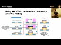 HIG Summit Presentation by Dr. Subodh Kulkarni
 Q&A; Wafer-Level and Advanced Packaging Inspection and Metrology | CyberOptics
 ReticleSense® Auto Teaching System™ ATSR
 SQ3000™ CMM | CyberOptics Industrial Metrology
 CyberOptics' CX150i Conformal Coating Inspection System In Action
 Application Uses for ReticleSense(TM) & WaferSense(R) Wireless Measurement Devices
 WaferSense® Auto Vibration System - AVS | CyberOptics Semiconductor