How Photolithography works | Part 1/6 – Introduction
Bernd Geh | The Key of Micro- and Nanoelectronics: Basics of Photolithography
Optics is a key technology with inspiring applications – such as in the production of increasingly powerful microchips. As a global technology leader in lithography optics and equipment, ZEISS is shaping the nanoelectronics age. This way ZEISS enables the continuation of Moore‘s Law, and with that the steady progress of the semiconductor industry.
Learn key aspects of the world of advanced optics for nanoelectronics in this recording of Bernd Geh’s talk on “The Key of Micro- and Nanoelectronics”. The six videos will give you an insight into the Basics of Photolithography. The learning videos are triggered by the Important Project of Common European Interest (IPCEI).
► Part 1: Introduction
• General introduction into the semiconductor industry
• Moore‘s Law and economic implications
► Part 2: Photolithography Basics: https://youtu.be/PsaOWZv9vH0
► Part 3: Photoresist: https://youtu.be/4ch1xFpMers
► Part 4: Imaging Process: https://youtu.be/VcBl6yhFrDo
► Part 5: Metrics for Lithography: https://youtu.be/VL0AaIDPDCg
► Part 6: Resolution Enhancement: https://youtu.be/H6iL_oE6z5A
► For more upcoming videos subscribe to the ZEISS YouTube Channel: https://zeiss.ly/youtube-subscribe
Видео How Photolithography works | Part 1/6 – Introduction канала ZEISS Group
Показать
Комментарии отсутствуют
Информация о видео
Другие видео канала
 How Photolithography works | Part 2/6 – Photolithography Basics
 A visit to ASML's cleanroom for EUV
 30 Years of ASML - From Shed To World Leader
 Pressure + Ink: Lithography Process
 EUV: Lasers, plasma, and the sci-fi tech that will make chips faster | Upscaled
 Photolithography
 How Photolithography works | Part 4/6 – Imaging Process
 Electron Beam Lithography
 From the ASML archives: "PAS 5500 - The Inside Story" (1993)
 How does Bluetooth Work?
 ASML - Powering the Next Phase of Semiconductor Manufacturing
 Breaking the Wall of EUV Lithography
 Why making chips is so hard
 How Photolithography works | Part 6/6 – Resolution Enhancement
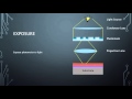 Photolithography: Step by step
 How Extreme Ultraviolet Lithography works | Part 1/3
 Inside The Worlds Largest Semiconductor Factory - BBC Click
 How ASML Builds a $150 Million EUV Machine
 Samsung Foundry vs TSMC
 Chip Manufacturing - How are Microchips made? | Infineon