- Популярные видео
- Авто
- Видео-блоги
- ДТП, аварии
- Для маленьких
- Еда, напитки
- Животные
- Закон и право
- Знаменитости
- Игры
- Искусство
- Комедии
- Красота, мода
- Кулинария, рецепты
- Люди
- Мото
- Музыка
- Мультфильмы
- Наука, технологии
- Новости
- Образование
- Политика
- Праздники
- Приколы
- Природа
- Происшествия
- Путешествия
- Развлечения
- Ржач
- Семья
- Сериалы
- Спорт
- Стиль жизни
- ТВ передачи
- Танцы
- Технологии
- Товары
- Ужасы
- Фильмы
- Шоу-бизнес
- Юмор
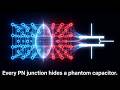
Biased p-n Junctions & The Diode Equation Explained | Solid State Devices Day 9 (B.Tech ECE)
Welcome to Day 9 of our 40-Day Solid State Devices series, designed specifically for B. Tech ECE students! Continuing with Module 2, we shift our focus from equilibrium conditions to "Biased p-n Junctions and the Diode Equation." In this episode, we explore the dynamic behavior of p-n junctions under both forward and reverse bias conditions. Discover how an applied external voltage either shrinks the depletion region to allow majority carrier flow (forward bias) or widens the barrier to block it (reverse bias). Finally, we provide a comprehensive qualitative and quantitative breakdown of William Shockley's Ideal Diode Equation. Whether you are studying for your university exams or building a foundation for VLSI design, this video is crucial for mastering real-world diode behavior!
Hashtags: #PNJunction, #ForwardBias, #ReverseBias, #ShockleyEquation, #IdealDiodeEquation, #SolidStateDevices, #SemiconductorPhysics, #BTech, #ECE, #ElectronicsEngineering
Disclaimer: Please note that this video contains AI-generated images, script, and voiceover.
Видео Biased p-n Junctions & The Diode Equation Explained | Solid State Devices Day 9 (B.Tech ECE) канала Flirting with Technology
Flirting with Technology Technology DIY Electronics Electrical Engineering How-to Earthing Grounding Earthing with multimeter Electrical safety Ground wire Earth leakage Transformer Delta-star transformer Autotransformer Voltage transformer Power system Electrical power Energy meter Digital energy meter Circuit breaker RCCB ELCB Miniature circuit breaker Induction motor AC motor Single-phase motor Voltage stabilizer Air conditioner Smoke alarm
Комментарии отсутствуют
Информация о видео
16 июня 2026 г. 17:54:32
00:02:07
Другие видео канала