Introduction to 555 Timer: The Internal Block Diagram and the Pin Diagram Explained
In this video, the brief introduction to the 555 Timer IC has been given and the pin diagram (of 8 pin DIP 555 IC) and the internal block diagram of the 555 timer have been explained.
By watching this video you will learn the following topics:
0:20 Introduction and Application of 555 timer IC
0:50 Pin Diagram of 555 Timer IC
1:06 Internal Block Diagram of 555 Timer
1:48 Brief description of 8 Pins and basic working of the internal blocks of 555 timer
what is 555 Timer IC?
The 555 timer IC is a very popular timer IC and it is widely used in many timing related applications.
It can be used as an oscillator, LED Flasher, tone generator, Frequency division, and timing delay generation.
The 555 timer IC is available in many packages but most popular is 8 pin DIP (Dual Inline Package).
The following is the list of the individual pin of 555 timer IC.
1. Ground
2. Trigger
3. Output
4. Reset
5. Control
6. Threshold
7. Discharge
8. Vcc
In this video, the brief description of each pin is given.
If you see the internal block diagram of 555 timer IC then it consists of the following parts.
1. Voltage Divider Circuit
2. Comparator
3. SR Flip-Flop
4. Discharge Circuit
5. Output Driver Circuit
In this video, the function of each block is explained in detail.
By connecting the external resistors and capacitor to the different pin of this 555 timer IC, it can be configured as either Astable, Monostable or Bistable Multivibrator and can be used in wide range of timing related applications.
This video will be helpful to all the students of science and engineering in understanding the basic working of 555 timer IC.
#555Timer
#PinDiagram
#InternalBlockDiagram
Follow me on YouTube:
https://www.youtube.com/allaboutelectronics
Follow me on Facebook:
https://www.facebook.com/ALLABOUTELECRONICS/
Follow me on Instagram:
https://www.instagram.com/all_about.electronics/
Music Credit:
http://www.bensound.com/
Видео Introduction to 555 Timer: The Internal Block Diagram and the Pin Diagram Explained канала ALL ABOUT ELECTRONICS
Показать
Комментарии отсутствуют
Информация о видео
18 сентября 2018 г. 16:58:29
00:11:33
Другие видео канала
 Monostable Multivibrator using 555 Timer Explained (with Working, Applications and Derivation)
 How 555 timers Work - The Learning Circuit
 Zener Diodes
 What is Multivibrator ? Astable, Monostable and Bistable Multivibrators Explained
 555 ic set Reset switch circuit
 How a quartz watch works - its heart beats 32,768 times a second
 How a 555 Timer IC Works
 Introduction To IC 555 Timer || in Hindi
 Electronic Basics #26: 555 Timer IC
 Basics and Block Diagram of Timer IC 555 - Special Purpose Integrated Circuits
 555 Timer as Astable Multivibrator (Working, Design and Derivations)
 Internal circuit of 555 timer | NE555 internal circuit explained
 3 Amazing Projects Using 555 Timer IC
 555 Timer Modes Explained - The Learning Circuit
 What is Phase Lock Loop (PLL)? How Phase Lock Loop Works ? PLL Explained
 555 Timer All Modes
 What is 555 Timer IC | 555 Timer Working | Internal Circuit of 555 Timer
 555 TIMER IC | Analog Devices & Circuits | Malayalam |
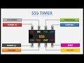 What is 555 timer?