- Популярные видео
- Авто
- Видео-блоги
- ДТП, аварии
- Для маленьких
- Еда, напитки
- Животные
- Закон и право
- Знаменитости
- Игры
- Искусство
- Комедии
- Красота, мода
- Кулинария, рецепты
- Люди
- Мото
- Музыка
- Мультфильмы
- Наука, технологии
- Новости
- Образование
- Политика
- Праздники
- Приколы
- Природа
- Происшествия
- Путешествия
- Развлечения
- Ржач
- Семья
- Сериалы
- Спорт
- Стиль жизни
- ТВ передачи
- Танцы
- Технологии
- Товары
- Ужасы
- Фильмы
- Шоу-бизнес
- Юмор
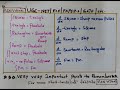
8086 General Bus Operation Timing Diagram | Memory Read & Write Cycle.
In this video, we clearly explain the 8086 General Bus Operation Timing Diagram, covering both Memory Read Cycle and Memory Write Cycle.
You will understand the role of CLK, ALE, RD, WR, DEN, AD0–AD15, A16–A19, and status signals S0–S7 with proper timing waveforms.
This explanation is very useful for:
ECE students
Microprocessors & Microcontrollers (8086)
GATE & University exams
Interview preparation
Watch till the end for an easy and exam-oriented understanding of 8086 bus timing diagrams.
Видео 8086 General Bus Operation Timing Diagram | Memory Read & Write Cycle. канала ASN Vision
8086 timing diagram 8086 general bus operation memory read cycle 8086 memory write cycle 8086 8086 microprocessor microprocessors and microcontrollers ECE microprocessor 8086 ALE signal 8086 RD WR signals AD0 AD15 multiplexed bus A16 A19 status signals 8086 S0 S1 S2 8086 DEN signal 8086 exam questions 8086 timing diagram explanation microprocessor timing diagrams ECE VLSI engineering microprocessors GATE microprocessors BTech ECE
Комментарии отсутствуют
Информация о видео
28 декабря 2025 г. 20:27:56
00:10:45
Другие видео канала